car obd2 tools
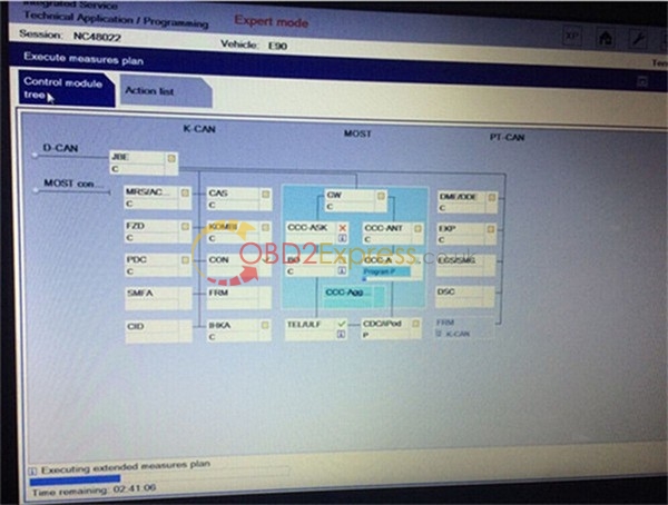
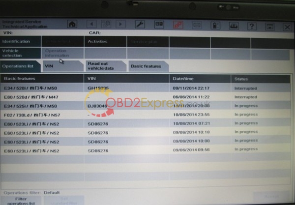
2015.12 ICOM software ISTA-D 3.56 ISTA-P 3.57 Advantages
Here’s the advantage list/ top reasons for BMW ISTA-D 3.56.1.002 ISTA-P 3.57.2.002 for ICOM A, A2, A3 interface.
2015.12 BMW ICOM Software Advantages:
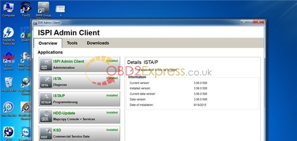
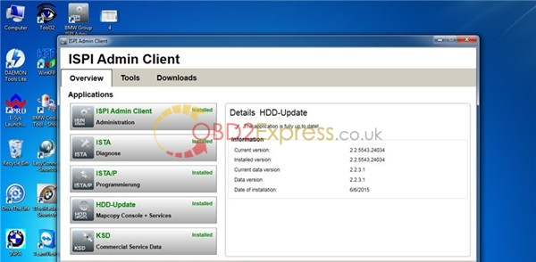
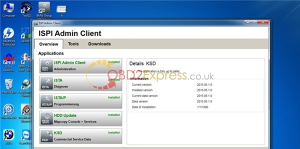
1. The 2015.12 Rheingold HDD has been updated to the newest R2 version, which boasts better efficiency, stability and performance than other R1 version HDDs
2. Support Multi-language: American English, British English, German, Spanish, French, Italian, polish, Portuguese, Turkish, Czech, Swedish, Dutch, Indian, Greek, Russian, Simplified Chinese, Traditional Chinese, Japanese, Korean and Thai.
3. Support almost 95% laptop on the world with Intel chip( I3/I5/I7 series) & Windows xp/ 7/8 OS and have 4GB memory, like Dell d630.
4. 2015 HDD can works with for BMW for ICOM, ICOM A2, ICOM A3 emulator.
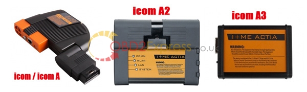
PS. Differences between BMW ICOM A1, A2 and A3
5. Software contain TIS and WDS software (for repair instruction and circuit).
6. No USB Dongle, no need to worry anymore for losting usb dongle will shut down your software.
7. Provide bonus engineer software for free, you can use it to do single module programming.
8. Support for BMW Engineers programming. (Expert Mode)
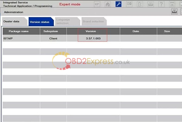
9. Support all BMW vehicles till the 2015 year
10. Customer review on real operation of 2015.12 Rheingold
09.03.2016. u 06:53 | 0 Komentara | Print | # | ^
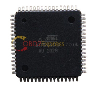
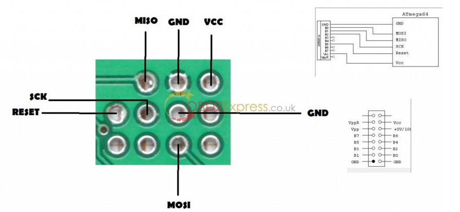
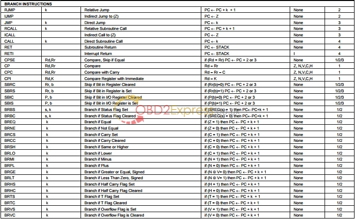
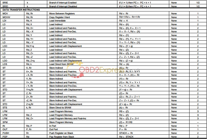
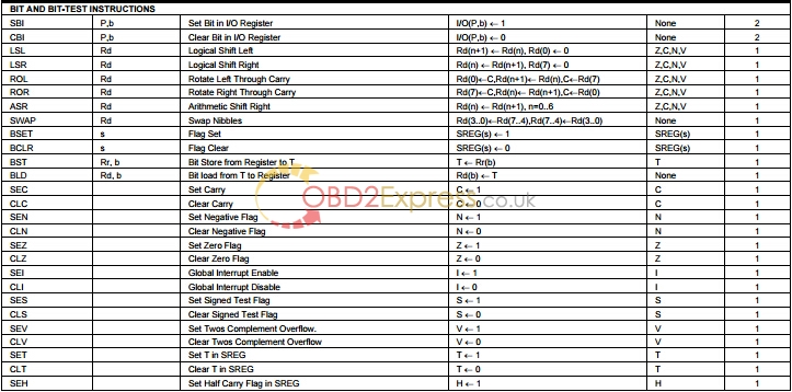
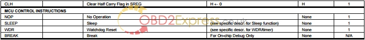
ATMEGA64 Repair Chip for Xprog-m User Manual
This is the user manual of ATMEGA64 Repair Chip which can help you update the XPROG-M programmer from V5.0 or V5.3 to V5.55, no dongle needed, full authorization support, including CAS4!
Main parts in the manual:
ATmega103 and ATmega64 Compatibility
ATMEGA64 Repair Chip Features
• High-performance, Low-power AVR® 8-bit Microcontroller
• Advanced RISC Architecture
– 130 Powerful Instructions – Most Single Clock Cycle Execution
– 32 x 8 General Purpose Working Registers + Peripheral Control Registers
– Fully Static Operation
– Up to 16 MIPS Throughput at 16 MHz
– On-chip 2-cycle Multiplier
• Non-volatile Program and Data Memories
– 64K Bytes of In-System Reprogrammable Flash
Endurance: 10,000 Write/Erase Cycles
– Optional Boot Code Section with Independent Lock Bits
In-System Programming by On-chip Boot Program
True Read-While-Write Operation
– 2K Bytes EEPROM
Endurance: 100,000 Write/Erase Cycles
– 4K Bytes Internal SRAM
– Up to 64K Bytes Optional External Memory Space
– Programming Lock for Software Security
– SPI Interface for In-System Programming
• JTAG (IEEE std. 1149.1 Compliant) Interface
– Boundary-scan Capabilities According to the JTAG Standard
– Extensive On-chip Debug Support
– Programming of Flash, EEPROM, Fuses, and Lock Bits through the JTAG Interface
• Peripheral Features
– Two 8-bit Timer/Counters with Separate Prescalers and Compare Modes
– Two Expanded 16-bit Timer/Counters with Separate Prescaler, Compare Mode, and Capture Mode
– Real Time Counter with Separate Oscillator
– Two 8-bit PWM Channels
– 6 PWM Channels with Programmable Resolution from 1 to 16 Bits
– 8-channel, 10-bit ADC
8 Single-ended Channels
7 Differential Channels
2 Differential Channels with Programmable Gain (1x, 10x, 200x)
– Byte-oriented Two-wire Serial Interface
– Dual Programmable Serial USARTs
– Master/Slave SPI Serial Interface
– Programmable Watchdog Timer with On-chip Oscillator
– On-chip Analog Comparator
• Special Microcontroller Features
– Power-on Reset and Programmable Brown-out Detection
– Internal Calibrated RC Oscillator
– External and Internal Interrupt Sources
– Six Sleep Modes: Idle, ADC Noise Reduction, Power-save, Power-down, Standby and Extended Standby
– Software Selectable Clock Frequency
– ATmega103 Compatibility Mode Selected by a Fuse
– Global Pull-up Disable
• I/O and Packages
– 53 Programmable I/O Lines
– 64-lead TQFP and 64-pad MLF
• Operating Voltages
– 2.7 - 5.5V for ATmega64L
– 4.5 - 5.5V for ATmega64
• Speed Grades
– 0 - 8 MHz for ATmega64L
– 0 - 16 MHz for ATmega64
ATMEGA64 update chip pinout
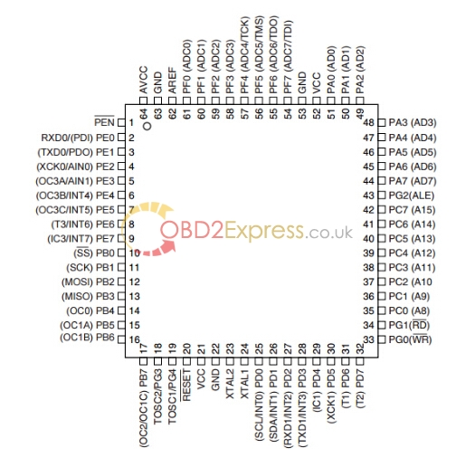
ATMEGA64 for Xprog M ECU programmer pinout:
Block Diagram
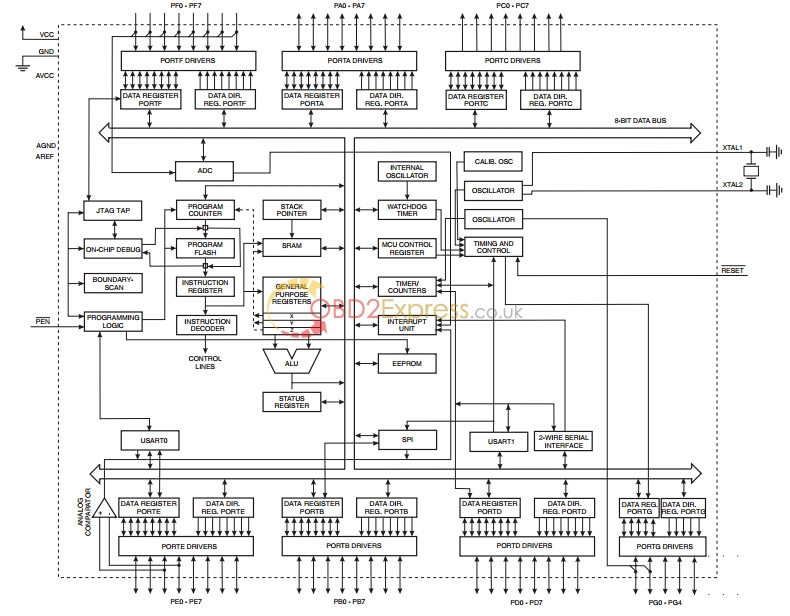
The AVR core combines a rich instruction set with 32 general purpose working registers. All the 32 registers are directly connected to the Arithmetic Logic Unit (ALU), allowing two independent registers to be accessed in one single instruction executed in one clock cycle. The resulting architecture is more code efficient while achieving throughputs up to ten times faster than conventional CISC microcontrollers.
The ATmega64 provides the following features: 64K bytes of In-System Programmable Flash with Read-While-Write capabilities, 2K bytes EEPROM, 4K bytes SRAM, 53 general purpose I/O lines, 32 general purpose working registers, Real Time Counter (RTC), four flexible Timer/Counters with compare modes and PWM, two USARTs, a byte oriented Two-wire Serial Interface, an 8-channel, 10-bit ADC with optional differential input
stage with programmable gain, programmable Watchdog Timer with internal Oscillator,an SPI serial port, IEEE std. 1149.1 compliant JTAG test interface, also used for accessing the On-chip Debug system and programming, and six software selectable power saving modes. The Idle mode stops the CPU while allowing the SRAM,Timer/Counters, SPI port, and interrupt system to continue functioning. The Powerdown mode saves the register contents but freezes the Oscillator, disabling all other chip functions until the next interrupt or Hardware Reset. In Power-save mode, the asynchronous timer continues to run, allowing the user to maintain a timer base while the rest of the device is sleeping. The ADC Noise Reduction mode stops the CPU and all I/O modules except asynchronous timer and ADC, to minimize switching noise during ADC conversions. In Standby mode, the crystal/resonator Oscillator is running while the rest of the device is sleeping. This allows very fast start-up combined with low power consumption. In Extended Standby mode, both the main Oscillator and the asynchronous timer continue to run.
The device is manufactured using Atmel’s high-density non-volatile memory technology. The On-chip ISP Flash allows the program memory to be reprogrammed In-System through an SPI serial interface, by a conventional non-volatile memory programmer, or by an On-chip Boot program running on the AVR core. The Boot Program can use any interface to download the Application Program in the Application Flash memory. Software in the Boot Flash section will continue to run while the Application Flash section is
updated, providing true Read-While-Write operation. By combining an 8-bit RISC CPU with In-System Self-Programmable Flash on a monolithic chip, the Atmel ATmega64 is a powerful microcontroller that provides a highly-flexible and cost-effective solution to many embedded control applications.
The ATmega64 AVR is supported with a full suite of program and system development tools including: C compilers, macro assemblers, program debugger/simulators, In-Circuit Emulators, and evaluation kits.
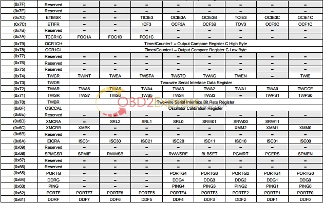
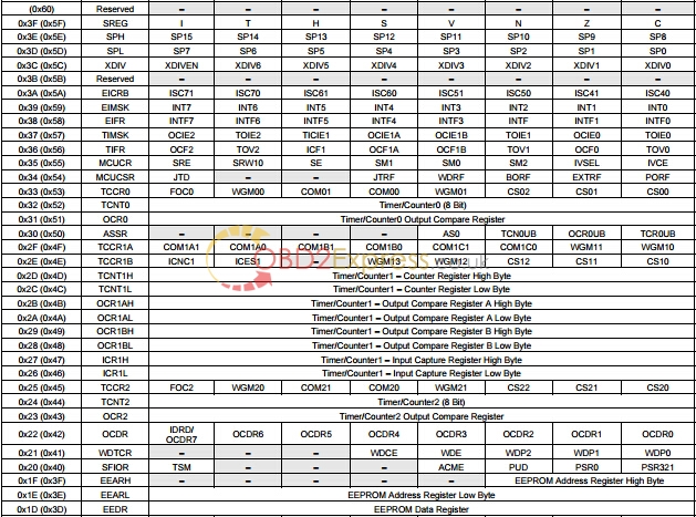
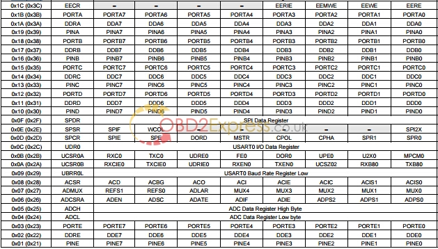
ATmega103 and ATmega64 Compatibility
The ATmega64 chip is a highly complex microcontroller where the number of I/O locations supersedes the 64 I/O location reserved in the AVR instruction set. To ensure backward compatibility with the ATmega103, all I/O locations present in ATmega103 have the same location in ATmega64. Most additional I/O locations are added in an Extended I/O space starting from 0x60 to 0xFF (i.e., in the ATmega103 internal RAM space). These location can be reached by using LD/LDS/LDD and ST/STS/STD instructions only, not by using IN and OUT instructions. The relocation of the internal RAM space may still be a problem for ATmega103 users. Also, the increased number of Interrupt Vectors might be a problem if the code uses absolute addresses. To solve these problems, an ATmega103 compatibility mode can be selected by programming the fuse M103C. In this mode, none of the functions in the Extended I/O space are in use, so the internal RAM is located as in ATmega103. Also, the extended Interrupt Vectors are removed. The ATmega64 is 100% pin compatible with ATmega103, and can replace the ATmega103 on current printed circuit boards. The application note “Replacing ATmega103 by ATmega64” describes what the user should be aware of replacing the ATmega103 by an ATmega64.
By programming the M103C Fuse, the ATmega64 will be compatible with the
ATmega103 regards to RAM, I/O pins and Interrupt Vectors as described above. However, some new features in ATmega64 are not available in this compatibility mode, these features are listed below:
• One USART instead of two, asynchronous mode only. Only the eight least significant bits of the Baud Rate Register is available.
• One 16 bits Timer/Counter with two compare registers instead of two 16 bits Timer/Counters with three compare registers.
• Two-wire serial interface is not supported.
• Port G serves alternate functions only (not a general I/O port).
• Port F serves as digital input only in addition to analog input to the ADC.
• Boot Loader capabilities is not supported.
• It is not possible to adjust the frequency of the internal calibrated RC Oscillator.
• The External Memory Interface can not release any Address pins for general I/O, neither configure different wait states to different External Memory Address sections.
• Only EXTRF and PORF exist in the MCUCSR Register.
• No timed sequence is required for Watchdog Timeout change.
• Only low-level external interrupts can be used on four of the eight External Interrupt sources.
• Port C is output only.
• USART has no FIFO buffer, so Data OverRun comes earlier.
• The user must have set unused I/O bits to 0 in ATmega103 programs.
VCC
Digital supply voltage.
GND
Ground.
Port A (PA7..PA0)
Port A is an 8-bit bi-directional I/O port with internal pull-up resistors (selected for each bit). The Port A output buffers have symmetrical drive characteristics with both high sink and source capability. As inputs, Port A pins that are externally pulled low will source current if the pull-up resistors are activated. The Port A pins are tri-stated when a reset condition becomes active, even if the clock is not running.
Port B (PB7..PB0)
Port B is an 8-bit bi-directional I/O port with internal pull-up resistors (selected for each bit). The Port B output buffers have symmetrical drive characteristics with both high sink and source capability. As inputs, Port B pins that are externally pulled low will source current if the pull-up resistors are activated. The Port B pins are tri-stated when a reset condition becomes active, even if the clock is not running.
Port C (PC7..PC0)
Port C is an 8-bit bi-directional I/O port with internal pull-up resistors (selected for each bit). The Port C output buffers have symmetrical drive characteristics with both high sink and source capability. As inputs, Port C pins that are externally pulled low will source current if the pull-up resistors are activated. The Port C pins are tri-stated when a reset condition becomes active, even if the clock is not running. Port C also serves the functions of special features of the ATmega64. In ATmega103 compatibility mode, Port C is output only, and the port C pins are not tri-stated when a reset condition becomes active.
Port D (PD7..PD0)
Port D is an 8-bit bi-directional I/O port with internal pull-up resistors (selected for each bit). The Port D output buffers have symmetrical drive characteristics with both high sink and source capability. As inputs, Port D pins that are externally pulled low will source current if the pull-up resistors are activated. The Port D pins are tri-stated when a reset condition becomes active, even if the clock is not running.
Port E (PE7..PE0)
Port E is an 8-bit bi-directional I/O port with internal pull-up resistors (selected for each bit). The Port E output buffers have symmetrical drive characteristics with both high sink and source capability. As inputs, Port E pins that are externally pulled low will source current if the pull-up resistors are activated. The Port E pins are tri-stated when a reset condition becomes active, even if the clock is not running.
Port F (PF7..PF0)
Port F serves as the analog inputs to the A/D Converter. Port F also serves as an 8-bit bi-directional I/O port, if the A/D Converter is not used. Port pins can provide internal pull-up resistors (selected for each bit). The Port F output buffers have symmetrical drive characteristics with both high sink and source capability. As inputs, Port F pins that are externally pulled low will source current if the pull-up resistors are activated. The Port F pins are tri-stated when a reset condition becomes active, even if the clock is not running. If the JTAG interface is enabled, the pull-up resistors on pins PF7(TDI), PF5(TMS) and PF4(TCK) will be activated even if a reset occurs.
The TDO pin is tri-stated unless TAP states that shift out data are entered.
Port F also serves the functions of the JTAG interface.
In ATmega103 compatibility mode, Port F is an input port only.
Port G (PG4..PG0)
Port G is a 5-bit bi-directional I/O port with internal pull-up resistors (selected for each bit). The Port G output buffers have symmetrical drive characteristics with both high sink and source capability. As inputs, Port G pins that are externally pulled low will source
current if the pull-up resistors are activated. The Port G pins are tri-stated when a reset condition becomes active, even if the clock is not running.Port G also serves the functions of various special features.
In ATmega103 compatibility mode, these pins only serves as strobes signals to theexternal memory as well as input to the 32 kHz Oscillator, and the pins are initialized to PG0 = 1, PG1 = 1, and PG2 = 0 asynchronously when a reset condition becomes active, even if the clock is not running. PG3 and PG4 are Oscillator pins.
RESET
Reset input. A low level on this pin for longer than the minimum pulse length will generate a reset, even if the clock is not running. The minimum pulse length is given in Table 19 on page 50. Shorter pulses are not guaranteed to generate a reset.
XTAL1
Input to the inverting Oscillator amplifier and input to the internal clock operating circuit.
XTAL2
Output from the inverting Oscillator amplifier.
AVCC
AVCC is the supply voltage pin for Port F and the A/D Converter. It should be externally connected to VCC, even if the ADC is not used. If the ADC is used, it should be connected to VCC through a low-pass filter.
AREF
AREF is the analog reference pin for the A/D Converter.
PEN
This is a programming enable pin for the SPI Serial Programming mode. By holding this pin low during a Power-on Reset, the device will enter the SPI Serial Programming mode. PEN has no function during normal operation.
![]()
Notes:
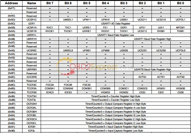
1. For compatibility with future devices, reserved bits should be written to zero if accessed. Reserved I/O memory addresses should never be written.
2. Some of the status flags are cleared by writing a logical one to them. Note that the CBI and SBI instructions will operate on all bits in the I/O Register, writing a one back into any flag read as set, thus clearing the flag. The CBI and SBI instructions work with registers 0x00 to 0x1F only
07.03.2016. u 07:46 | 0 Komentara | Print | # | ^
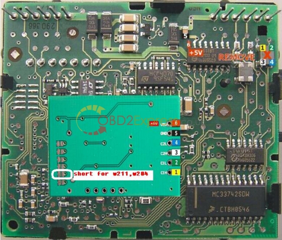
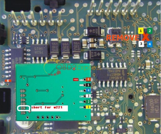
MB CAN Filter on Mercedes E-class W212 Connection Diagram
The Mercedes-Benz W221 model use the new EZS with the NEC processor marked JURA (also named EIS-electronic ignition switch). And Mercedes CAN filter will work with the EZS module. For installation remove EZS from car.
MB CAN filter to select:
MB CAN Filter 5 in 1 for W221 W204 W212 W166 and X166
MB CAN Filter 8 in 1 for W221 W204 W212 W166 and X166 W172 W218 W246
MB CAN Filter 12 in 1 for W221 W204 W207 W212 W166 X166 W218 W172 W246 W176 W117 W156
Step-by-step installation instruction:
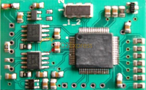
1- prepare Mercedes CAN filter board:
check - resistor 121 must be soldered and solder second configuration points like in pictures.
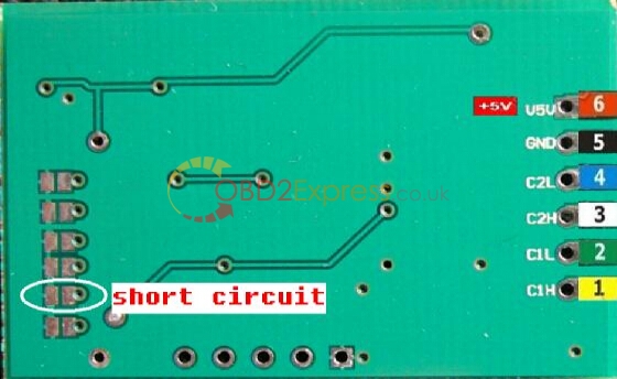
2- Remove from EZS board SMD part marked with red “X”.
With short, good isolated wire connect Mercedes CAN filter to EZS board according picture: 1-1 (C1H), 2-2(C1L), 3-3(C2H), 4-4(C2L), 5- 5(GND), and 6-6 (+5V).
Mercedes S-class W221 another type:
04.03.2016. u 07:20 | 0 Komentara | Print | # | ^
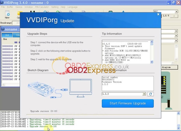
XHorse VVDI Prog programmer V4.3.1 software Free download
Original Xhorse VVDI PROG ECU/MCU/EEPROM programmer software has been updated to V4.3.1 in obdexpress.co.uk,Here is the information about the new VVDI PRO V4.3.1 Oznake: car diagnostic tool
Newest Software Version: V4.3.1
Newest Hardware Version: V1.2.2
Free download VVDI-PROG V4.3.1
https://mega.nz/#!oxhilR7S!TqaQG7_1vUfdOnAOh00dYiioePGapUMcA46PR1Mu4a0
What’s new in VVDI PROG v4.3.1?
VVDIProg v4.3.1 (2016-01-27)
* This version DON't need update
firmware
+ Add MC9S12GN16_UNSECURED,
MC9S12GNA16_UNSECURED,
MC9S12GN32_UNSECURED,
MC9S12GNA32_UNSECURED,
MC9S12G48_UNSECURED,
MC9S12GA48_UNSECURED,
MC9S12GN48_UNSECURED,
MC9S12G64_UNSECURED,
MC9S12GA64_UNSECURED,
MC9S12G96_UNSECURED,
MC9S12GA96_UNSECURED,
MC9S12G128_UNSECURED,
MC9S12GA128_UNSECURED,
MC9S12G192_UNSECURED,
MC9S12GA192_UNSECURED,
MC9S12G240_UNSECURED,
MC9S12GA240_UNSECURED options
Mask:(0N95B,0N51A,0N75C,1N75C,
0N48A,1N48A)
MC9S12HA32_UNSECURED,
MC9S12HA48_UNSECURED,
MC9S12HA64_UNSECURED,
MC9S12HY32_UNSECURED,
MC9S12HY48_UNSECURED,
MC9S12HY64_UNSECURED options
Mask:(0M34S)
MC9S12P32_UNSECURED,
MC9S12P64_UNSECURED,
MC9S12P96_UNSECURED,
MC9S12P128_UNSECURED options
Mask:(0M01N)
MC9S12XEA128_UNSECURED,
MC9S12XEG128_UNSECURED,
MC9S12XEA128_SECURED,
MC9S12XEG128_SECURED options
Mask:(1M53J,2M53J,0N36H,1N36H)
MC9S12XHY128_UNSECURED,
MC9S12XHY256_UNSECURED options
Mask:(0M23Y)
MC9S12XS64_UNSECURED,
MC9S12XS128_UNSECURED,
MC9S12XS256_UNSECURED options
Mask:(0M04M,1M04M,0M05M)
in <2-MCU>->
+ Add MC9S12XE_UNLOCK option
in <2-MCU>->
(Backup all data before use it)
+ Add ME20U2-XET256-BACKUP,
ME20U2-XET512-BACKUP,
MT22-XEP768-BACKUP,
MT60-XEP768-BACKUP options
in <3-ECU>->
+ Add the 12V power adaptor status
in information dialog
How to update Xhorse VVDI-PROG VVDI PROG super programmer:
1) Connect the device with the USB wire for the computer
2) Click on the following start online upgrade button to upgrade
3) Waiting for the upgrade to complete