Over the years, technology has obviously advanced in ways that can be helpful to people's everyday lives. Unevitably, it also comes with different risks.Whether they know it or not, nearly everyone relies on technology every day. Today, technology is used by even the most important people/organizations in the U.S., such as Homeland Security. That is why cybersecurity is very important to anyone who uses technology. Oznake: Cybersecurity
Cybersecurity itself is actions taken to prevent any problems we may have with unwanted people seeing or even stealing anything on our technology devices. The more technology advances the more security we need to have. A weak cyber security system can result in other countries hacking into U.S. systems, networks, programs, devices, and data. This poses a great threat to our national security.
We may be able to help the issue if major cybersecurity companies such as Homeland security could help spread the awareness to the U.S. We could even take it a step further and send out security packages that Microsoft has been selling since the hack.
Spreading awareness is the fastest and most effective way of letting people know how and what to do in this type of situation. Another reason is because spreading awareness doesn´t always cost a lot of money if any. This information can be disseminated to anyone of all ages, and let everyone know about what cyber security is.
A large number of people may think that their cybersecurity is fine, but did you know that cyber attacks have risen by 35% since 2020? Last year, the U.S. government alone had 28,581 cases of hacked data. Outside of the government cyber security, cyber attacks in general have gone up 180% in the last couple of years. These statistics do not include the American population which has about once every 11 seconds. Considering 7,240 of the 28,581 cyber attacks went unknown this last year should motivate people to take in some cyber knowledge.
Warning Americans and spreading awareness will help reduce the percentage or prevent internet attacks from increasing. Making U.S internet environment safer will not only protect citizens but all their information on the internet too. Providing information about cybersecurity to everyone who works from school to office helps protect the online world from everyone around us and keeps us one step ahead.
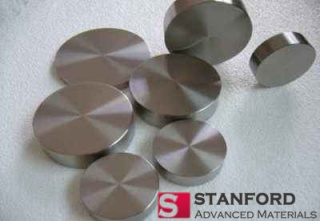
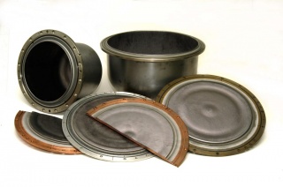
Information from Stanford Advanced Materials.
CITATIONS
Johnson, Joseph. "U.S. Government Cyber Security Incidents by Attack Vector 2019." Statista. 11 Feb. 2021. Web. 30 Aug. 2021.
Allen, Josh, Josh Allen, Reviewed by Jason Firch. "Recent Cyber Attacks
Americans Need to Know More About Cyber Security
20 listopad 2021komentiraj (0) * ispiši * #
Core technology of semiconductor sputtering target
25 prosinac 2019The semiconductor industry is a high-tech industry with high technological thresholds and high output values. The output value of the global semiconductor industry this year is expected to reach 500 billion US dollars. Semiconductor manufacturing not only requires advanced lithography machines, but materials are also an important part of it, mainly including silicon wafers, photoresists, high-purity reagents, CMP materials, and sputtering targets.
High-purity metal sputtering targets mainly refer to metal targets with a purity of 99.9% -99.999%. They are used in the physical vapor deposition (PVD) process of electronic component manufacturing and are the key materials for the preparation of electronic thin films.
Sputtering is one of the main techniques for preparing thin-film materials. It uses the ions generated by the ion source to accumulate in a vacuum to form a high-speed energy ion beam, which bombards the solid surface, and the atoms on the solid surface leave the solid and are deposited on the substrate surface. The bombarded solid is the raw material for the thin film deposition by sputtering, which is called sputter coater target.
There are four main types of metal sputtering targets produced by Stanford Advanced Materials (SAM): aluminum, titanium, tantalum, and tungsten titanium targets. In addition, the company's other products include copper targets, nickel targets, cobalt targets, chromium targets, ceramic targets and other sputtering targets, as well as metal evaporation materials, carbon fiber composite parts for LCDs (mainly including carbon fiber support, carbon fiber drive shaft , Carbon fiber fork arm), etc. At the same time, the company sells tantalum targets (including tantalum rings) and titanium targets (including titanium rings) recovered from customers, and provides customers with cleaning and refurbishing services.
Here are 6 important facts about semiconductor wafers:
- Semiconductor is a solid substance whose conductivity is between insulator and metals, either due to the addition of an impurity or because of temperature effects. In other words, the conductivity of the semiconductor can be controlled by adding impurities as a specific amount of other materials to the semiconductor.
- Most semiconductor wafers are made of silicon, which is the second-most abundant element in the Earth's crust. In addition to silicon, semiconductors also use other materials, including germanium, gallium arsenide, germanium, indium phosphide, sapphire and quartz.
- Semiconductor wafers are available in a spread of diameters. The first semiconductor wafer made inside the US in 1960 was just 1 inch in diameter. Today, standard semiconductor wafers go up to 12 inches to 18 inches.
- Water is the key component of manufacturing silicon wafers. It is a compound that basically is a general solvent for all substances, silicon included. A large production facility uses up to 4.8 million gallons of water every day to supply Silicon wafers for manufacturing needs and supply.
- The thickness of semiconductor wafers varies greatly. The thickness of the wafer is always determined by the mechanical strength of any material used to make it. Regardless of what the semiconductor is made of, the wafer must be thick enough to support its own weight so that it does not break during processing.
- Contamination is inevitable during the manufacture and transportation of semiconductors. Appropriate storage conditions must be in place to prevent contamination and/or degradation after shipment. Semiconductor wafers that are not vacuum sealed must be placed in a Nitrogen (N2) cabinet at a flow rate of 2 to 6 SCFH (Standard Cubic Feet per Hour).
Oznake: metal sputtering target, semiconductor, evaporation materials, sputter coater targets
komentiraj (0) * ispiši * #
Equipment for the Production of Different Sputtering Target Materials
08 kolovoz 2019The metal sputtering target requires a vacuum melting furnace, or a vacuum sintering furnace or a hydrogen atmosphere sintering furnace for sheet stamping; then a forging hammer and a rolling mill may be required for pressure forming; then a vacuum annealing furnace is required for heat treatment of the target; then the vacuum annealing furnace is needed to heat the target; then ultrasonic non-destructive testing equipment is needed for testing; then scanning electron microscope, ICP, laser particle size analyzer, Fisher's particle size analyzer, metallographic microscope and its sample preparation equipment are needed for chemical composition analysis, metallographic analysis, powder particle size analysis and even texture analysis; then a variety of turning and milling grinders are needed for machining; finally, the target packaging is also needed.
Non-metallic targets require the use of a sintering furnace. The rest of the equipment is the same as the metal sputtering target.
Some sintering furnaces have different atmospheres and may not be universal. For example, the sintering furnace for sintering tungsten and molybdenum is in a vacuum of 2200 degrees in a hydrogen or hydrogen atmosphere, the furnace for sintering the ITO target is in a 1500 degree in a pure oxygen atmosphere, and the one for sintering AZO ceramic sputter target is a kiln continuous sintering furnace in an atmospheric atmosphere.
In the case of aluminum alloy or copper alloy targets, vacuum melting and vacuum casting are generally used. For example, in the case of titanium alloy, it is generally the smelting and casting of a vacuum electron beam melting furnace. In addition, tungsten-molybdenum rotating targets are also used for hot isostatic pressing or hot extrusion, but are generally the most common for forging and rolling.
Generally, the ceramic powder is granulated and formed before sintering. Taking a sintered AZO target as an example, a spray dryer, a ball mill, a press and a steel mold, a cold isostatic press, and a rubber mold may be required. For another example, an ITO ceramic target may require a plaster mold, a slurry agitator, and the etc.
For more information, please visit https://www.sputtertargets.net/sputtering-target.html.
Oznake: sputtering target
komentiraj (0) * ispiši * #
Reactive Sputtering of Titanium Target
10 srpanj 2019Reactive sputtering is a common technique for preparing thin films of metal oxides, nitrides, and carbides. In this process, the metal sputtering target is sputtered in a mixture of argon and other reactive gases such as oxygen, nitrogen, methane, and the like. It is advantageous to use a metal target instead of a composite target because it is easier to process the metal, and its target sputtering rate is usually high and the thermal conductivity is good. In addition, complex compounds having polymetallic elements can also be produced using reactive sputtering of metal alloys or by co-sputtering from different elemental targets.
Although reactive sputtering is superior to composite sputtering, reactive sputtering is a nonlinear process and, in most cases, has a hysteresis effect due to target poisoning caused by the interaction of the target with the target and the reactive gas. It may cause charge accumulation and arc discharge. In addition, the sputtering yield is lowered because the binding energy between titanium and carbon atoms is higher than the binding energy between titanium atoms. The formation of a new layer on the surface of the titanium sputtering target results in a decrease in yield and deposition rate.
The synthesis of multi-component nanocomposite or functionally graded membranes by reactive sputtering requires critical control of process parameters. This is because electrical, optical, and mechanical properties can vary with film composition as process conditions change. There is a real need to control process parameters, particularly when it is desired to synthesize films with reproducible chemistries and when film growth occurs in so-called transition regions, with reference to the transition from metal to composite sputtering mode.
Titanium carbide (TiC) is a gap transition metal carbide. TiC and other interstitial carbides are characterized by high hardness, high melting point, low thermal conductivity and significant non-stoichiometry. All transition metal carbides have a very large range of stability and a large number of carbon vacancies. Thus, this formula is commonly written as TiCx, where x refers to the carbon moiety in the compound. The value of x can be varied without any structural change in the range of about 0.47-0.97. This provides considerable room for adjusting the physical properties of the film without structural changes.
Reactive sputtering of titanium targets in argon and methane is an attractive method for depositing Ti-C films having different compositions. However, due to changes in flow rate or partial pressure of methane gas, a sharp transition from metal to composite sputtering mode makes control of one or two parameters critical. Much research has been conducted to investigate the effects of overflow transitions between metal sputtering and reactive sputtering modes using elemental, binary, ternary and/or quaternary alloy targets in the presence of one or more reactive gases. . Various techniques have been used to deposit TiC films, including reactive sputtering, activation reaction evaporation, reactive pulsed laser deposition, and plasma arc deposition. However, there is currently no published study on the hysteresis behavior of direct current (DC) sputtered titanium targets in Ar/CH4 gas mixtures.
For more information, please visit https://www.sputtertargets.net/.
komentiraj (0) * ispiši * #
Four Kinds of Micro-arc Oxidation Method for Titanium Alloy Application
21 lipanj 2019Currently, composite coating technology will gradually replace single coating technology driven by the growing industrial demand. Micro-arc oxidation, also known as micro-plasma oxidation, can produce ceramic layers with good metallurgical properties on the surface of light metals Al, Mg, Ti and corresponding alloys by means of high voltage, high current and instantaneous high temperature. The main component of the ceramic layer is the oxide grown in situ in the matrix, and the electrolyte component is also involved in the micro-arc oxidation film layer. The electrical parameters (such as solution formulation, voltage and current, duty cycle, pulse frequency, etc.) in the micro-arc oxidation process have a great influence on the preparation and microstructure of the micro-arc oxidation film. The method is safe in process, simple in operation, environmentally friendly in solution, and has the advantages that the process which is unmatched by other processing technologies is simple, the film layer is uniform and compact, and the size of the workpiece is less restricted.
Related: Everything You Need to Know About Titanium Sputtering Target
Titanium alloy micro-arc oxidation film has the advantages of high hardness, high film-bonding strength, corrosion resistance and wear resistance, but the surface of the film is rough, loose and porous, and the friction coefficient is large, thus reducing the wear resistance of the film. It shortens the service life of the oxide film and is not conducive to the application of titanium alloy in the wear environment. At present, in order to improve the defect of titanium alloy micro-arc oxidation film, some research institutes of the Russian Academy of Sciences have carried out a lot of work, and the domestic concern about this issue has just started. This paper mainly introduces the related technology of composite processing based on micro-arc oxidation technology combined with sealing method, aluminum plating method, pulsed electron beam method, hydrothermal method and electrophoretic deposition method.
Micro-arc oxidation + sealing method
Due to the loose porous surface of the titanium alloy micro-arc oxidation film, some researchers have tried to fill the pores of the micro-arc oxide film by physical, chemical or electrochemical methods to achieve self-lubrication. Among them, polytetrafluoroethylene (PTFE) is an ideal self-lubricating material because of its good thermal stability and excellent chemical stability in various environments.
Micro-arc oxidation + hydrothermal method
In the hydrothermal method, a reaction medium is contained in a sealed container, and the container is continuously heated by a heat source to bring the inside of the container to a high temperature and a high pressure. Under the action of high temperature and high pressure, the insoluble or insoluble matter will dissolve and further recrystallize.
Microarc oxidation + pulsed electron beam
Pulsed electron beam (HCPEB) surface treatment technology uses high-speed electrons as a carrier to apply incident energy to the surface of the material in a very short time and causes a series of phenomena, including melting, condensation, vaporization, enhancement, diffusion, etc. Physical, chemical, and mechanical properties that are difficult to achieve with other heat treatments. The HCPEB method is used to prepare the composite modified layer on the titanium alloy micro-arc oxidation film, which belongs to the coating remelting category, that is, the micro-arc oxidation coating is prepared in advance, and then HCPEB is applied to the oxide film to perform electron beam remelting, thereby improving Uniform compactness of the film layer, degree of grain refinement, bond strength of the film base, wear resistance, corrosion resistance and the like.
Micro arc oxidation + aluminum plating
Related: Aluminum Titanium (Al/Ti) Sputtering Target
Compared with titanium alloys, aluminum alloys have many similar properties. For example, they are all valve metals, similar in application fields, low in density and high in specific strength. They are also widely used in metal fields. However, the properties of oxides of titanium alloys and aluminum alloys after micro-arc oxidation treatment vary greatly. The main composition of the oxide film formed by micro-arc oxidation of titanium alloy is TiO2 (rutile and anatase); the main products of micro-arc oxidation of aluminum alloy are Al2O3 (±-Al2O3 and ł-Al2O3). The hardness of Al2O3 is between 1200 and 1800 HV, which is significantly higher than the hardness of TiO2 (550~1050 HV). At the same time, the toughness of TiO2 is insufficient, and ł-Al2O3 has high structural and toughness. Therefore, in terms of hardness and wear resistance, the titanium alloy micro-arc oxidation film is not as good as the aluminum alloy micro-arc oxidation film.
For more information, please visit https://www.sputtertargets.net/.
komentiraj (0) * ispiši * #
Pozdrav, svima. Ja sam Julissa.
20 lipanj 2019Pozdrav svima, ja sam Julissa. Trenutno radim kao urednik u tvrtki za proizvodnju meta u SAD-u. Svrha ovog bloga je podijeliti neke praktične članke o metama prskanja i materijalima za isparavanje. Ako ste zainteresirani, slijedite me.
Oznake: sputtering target
komentiraj (0) * ispiši * #


